- 您现在的位置:买卖IC网 > Sheet目录2002 > ISL76161AVZ (Intersil)IC 12-BIT HS D/A 28-TSSOP
11
FN6720.2
December 23, 2013
Propagation Delay
The converter requires two clock rising edges for data to be
represented at the output. Each rising edge of the clock
captures the present data word and outputs the previous
data. The propagation delay is therefore 1/CLK, plus <2ns of
settling. See Figure 13.
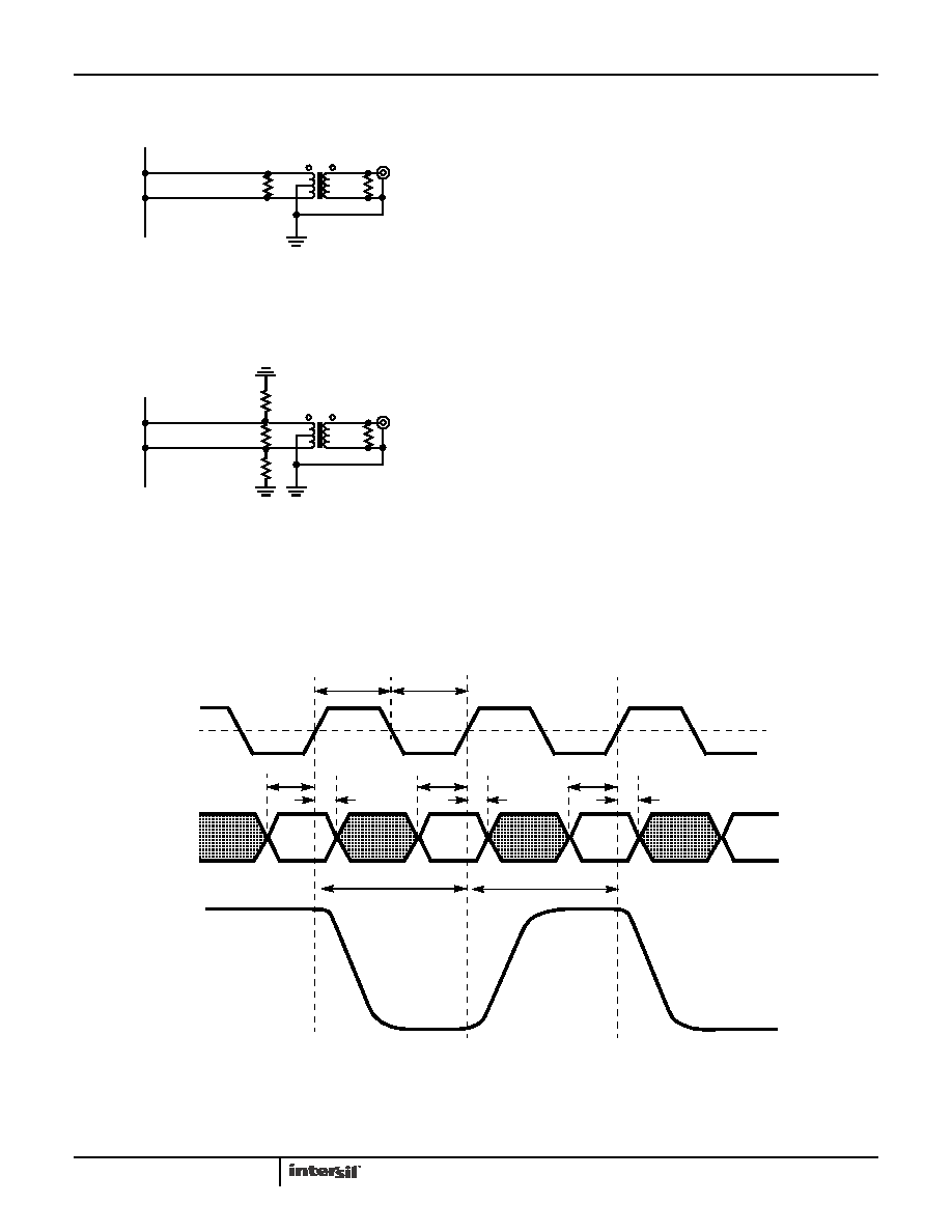
FIGURE 11. OUTPUT LOADING FOR DATASHEET
MEASUREMENTS
PIN 21
PIN 22
RDIFF
ISL76161
RLOAD
IOUTB
IOUTA
VOUT = (2 x IOUTA x REQ)V
LOAD SEEN BY THE TRANSFORMER
RLOAD REPRESENTS THE
1:1
REQ = 0.5 x (RLOAD // RDIFF)
AT EACH OUTPUT
FIGURE 12. ALTERNATIVE OUTPUT LOADING
PIN 21
PIN 22
ISL76161
IOUTB
IOUTA
VOUT = (2 x IOUTA x REQ)V
REQ = RA // [ 0.5 x (RLOAD // RDIFF) ], WHERE RA=RB
AT EACH OUTPUT
RLOAD
RDIFF
RA
RB
LOAD SEEN BY THE TRANSFORMER
RLOAD REPRESENTS THE
Timing Diagram
FIGURE 13. PROPAGATION DELAY, SETUP TIME, HOLD TIME AND MINIMUM PULSE WIDTH DIAGRAM
CLK
IOUT
50%
tPW1
tPW2
tSU
tHLD
tSU
tPD
tHLD
D11-D0
W0
W1
W2
W3
OUTPUT = W0
OUTPUT = W1
tPD
OUTPUT = W-1
ISL76161
发布紧急采购,3分钟左右您将得到回复。
相关PDF资料
ISL81387IAZ-T7A
IC TXRX RS232/485 DL ESD 20SSOP
ISL81485IU-T
IC TXRX RS485/422 5V HS 8-MSOP
ISL81486IU-T
IC TXRX RS485/422 5V HS 8-MSOP
ISL83075EIBZA
IC TXRX RS485/422 3.3V ESD 8SOIC
ISL83088EIU-T
IC TXRX RS485/422 5V ESD 8-MSOP
ISL83220EIV-T
IC 1DRVR/1RCVR RS232 16-TSSOP
ISL83384ECA-T
IC 2DRVR/2RCVR RS232 3V 20-SSOP
ISL83385EIB-T
IC 2DRVR/2RCVR RS232 3V 18-SOIC
相关代理商/技术参数
ISL76161AVZ-T
功能描述:IC CONV D/A 12BIT HS 28-TSSOP RoHS:是 类别:集成电路 (IC) >> 数据采集 - 数模转换器 系列:- 产品培训模块:Lead (SnPb) Finish for COTS
Obsolescence Mitigation Program 标准包装:1,000 系列:- 设置时间:1µs 位数:8 数据接口:串行 转换器数目:8 电压电源:双 ± 功率耗散(最大):941mW 工作温度:0°C ~ 70°C 安装类型:表面贴装 封装/外壳:24-SOIC(0.295",7.50mm 宽) 供应商设备封装:24-SOIC W 包装:带卷 (TR) 输出数目和类型:8 电压,单极 采样率(每秒):*
ISL76161AVZ-TK
功能描述:IC CONV D/A 12BIT HS 28-TSSOP RoHS:是 类别:集成电路 (IC) >> 数据采集 - 数模转换器 系列:- 产品培训模块:Lead (SnPb) Finish for COTS
Obsolescence Mitigation Program 标准包装:1,000 系列:- 设置时间:1µs 位数:8 数据接口:串行 转换器数目:8 电压电源:双 ± 功率耗散(最大):941mW 工作温度:0°C ~ 70°C 安装类型:表面贴装 封装/外壳:24-SOIC(0.295",7.50mm 宽) 供应商设备封装:24-SOIC W 包装:带卷 (TR) 输出数目和类型:8 电压,单极 采样率(每秒):*
ISL76321
制造商:INTERSIL 制造商全称:Intersil Corporation 功能描述:16-Bit Long-Reach Video Automotive Grade SERDES with Bi-directional Side-Channel
ISL76321ARZ
功能描述:串行器/解串器 - Serdes ISL76321 48L 7X7(PUN CHED AUTO RoHS:否 制造商:Texas Instruments 类型:Deserializer 数据速率:1.485 Gbit/s 输入类型:ECL/LVDS 输出类型:LVCMOS 输入端数量:1 输出端数量:20 工作电源电压:2.375 V to 2.625 V 工作温度范围:0 C to + 70 C 封装 / 箱体:TQFP-64
ISL76321ARZ-T13
功能描述:串行器/解串器 - Serdes ISL76321 48L 7X7(PUN CHED AUTO RoHS:否 制造商:Texas Instruments 类型:Deserializer 数据速率:1.485 Gbit/s 输入类型:ECL/LVDS 输出类型:LVCMOS 输入端数量:1 输出端数量:20 工作电源电压:2.375 V to 2.625 V 工作温度范围:0 C to + 70 C 封装 / 箱体:TQFP-64
ISL76321ARZ-TK
功能描述:串行器/解串器 - Serdes ISL76321 48L 7X7(PUN CHED 1K AUTO RoHS:否 制造商:Texas Instruments 类型:Deserializer 数据速率:1.485 Gbit/s 输入类型:ECL/LVDS 输出类型:LVCMOS 输入端数量:1 输出端数量:20 工作电源电压:2.375 V to 2.625 V 工作温度范围:0 C to + 70 C 封装 / 箱体:TQFP-64
ISL76322
制造商:INTERSIL 制造商全称:Intersil Corporation 功能描述:16-Bit Long-Reach Video Automotive Grade SERDES
ISL76322_1108
制造商:INTERSIL 制造商全称:Intersil Corporation 功能描述:16-Bit Long-Reach Video Automotive Grade SERDES